Challenge
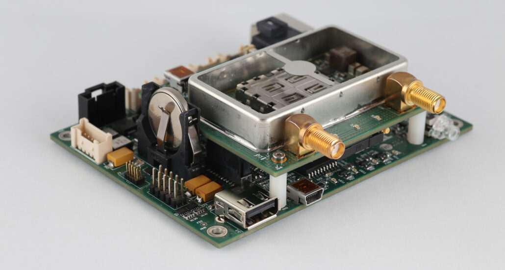
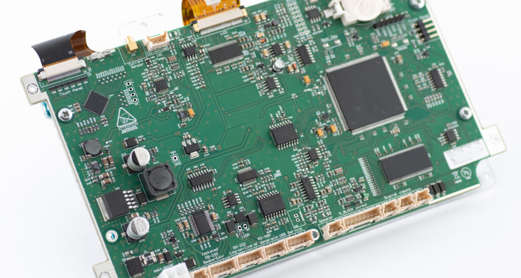
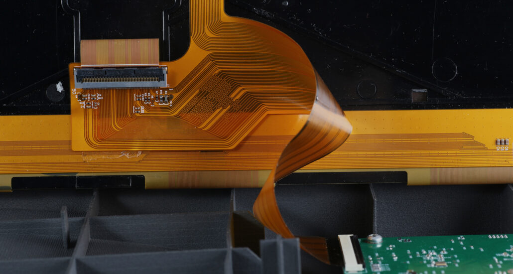
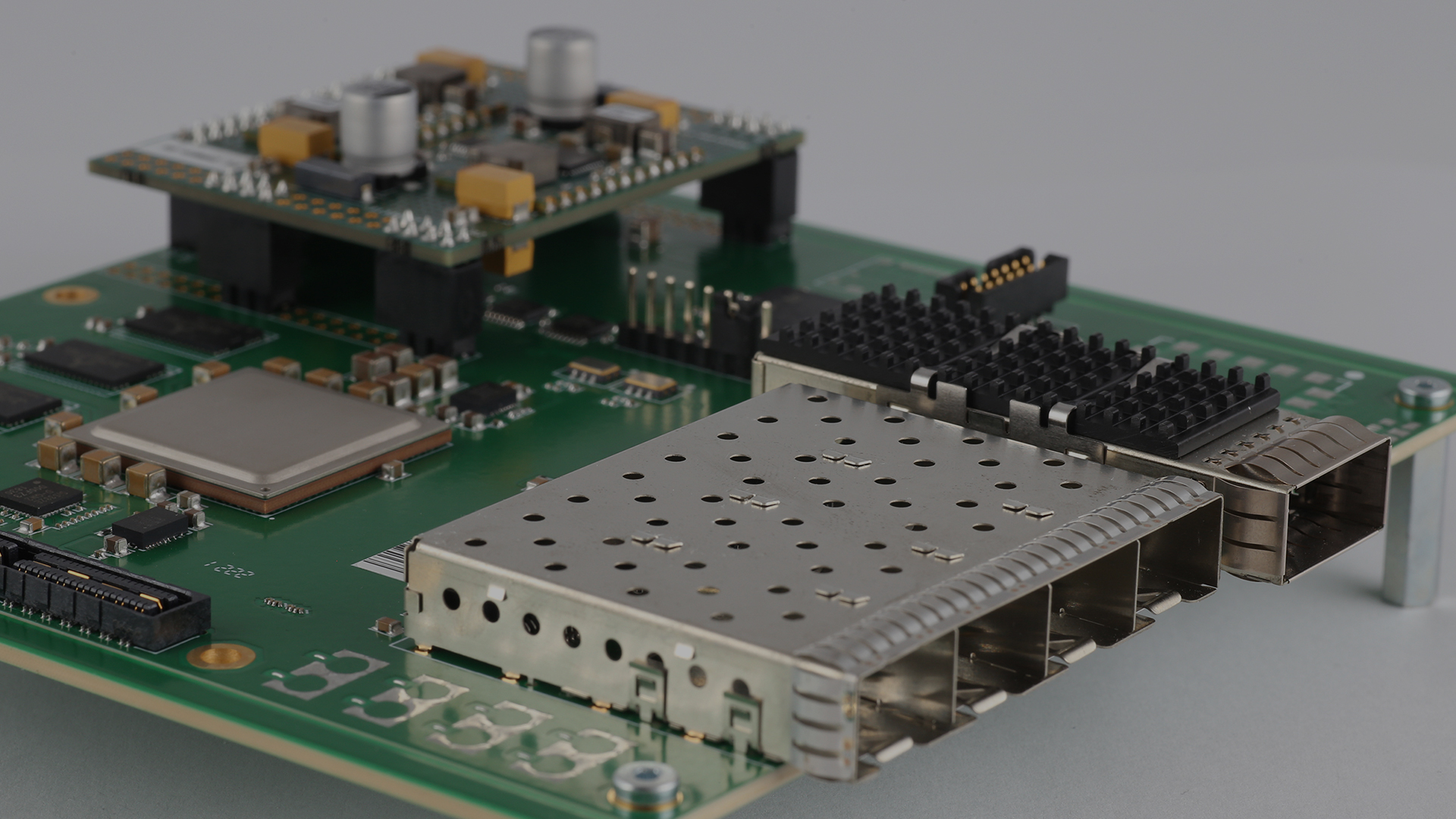
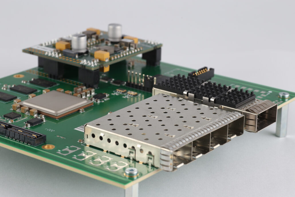
This project concerned verification of the design process of electronic devices, containing ultra-fast digital interfaces. The overriding requirement was to extend the design process with broadband simulations of signal integrity and power (SI/PI) phenomena, as well as to select and verify the instruments, in order, subsequently, to verify the measurements. The key elements of the project were an impedance coupon (IC) design, containing selected, high-density routing elements, the so-called, HDI (High Density Interconnect), design of the Test System – an experimental electronic device, for the functional verification of SFP+, QSFP28 and DDR4 interfaces. As part of the project, simulations and measurements of the coupon and quick connections of the Test System were carried out, i.e. 25Gbps (NRZ) by transceivers using the integrated Xilinx Kintex Ultrascale+FPGA chip. The project was commissioned by one of the Polish telecommunications operators and was the technological reconnaissance phase for particularly advanced electronic projects.
“The biggest challenge of the project was the multi-gigabit interface speeds and the associated, very wide simulation and measurement bandwidth, reaching 40GHz. It was necessary to properly select the Instrumentation, taking into account not only the measuring devices themselves, but also the accessories and measuring methodologies necessary. The whole thing was to verify the accuracy of the simulator results against reality and confirm the correctness of the design process, which, ultimately, was successful.”
Kamil Grabowski, CEO
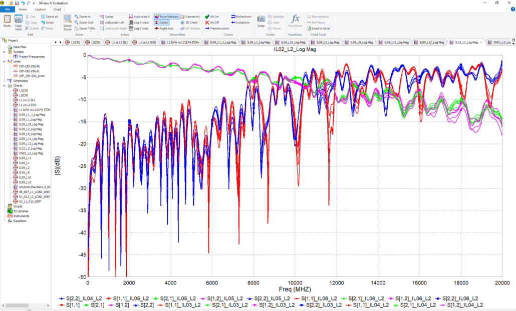
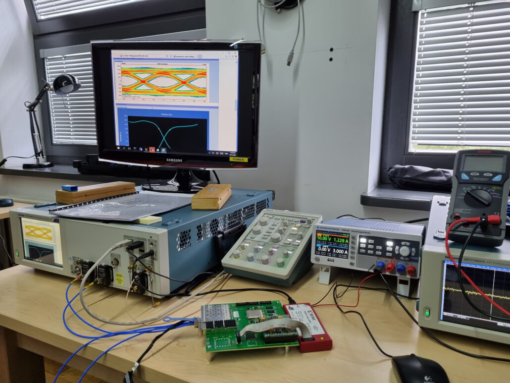
The project required a tremendous amount of work to acquire fundamentally new and advanced knowledge in a fairly short period of time. The identification of SI/PI simulation tools was carried out and functional simulations and extractions of the quadruple models of selected UT connections and IC test lines (mainly in Cadence Sigrity 2019) were also carried out. In order to confirm the physicality of the implementation of the interfaces, a fully functional electronic circuit was made, containing the FPGA Xilinx Kintex US+ system, enabling communication with transceivers, at a speed of 25Gbps. Advanced ISOLA materials were used for stack design and PCB fabrication. In the next steps, the UT was successfully launched, compliance with IEEE802.3 CAUI4 and JEDEC-DDR4 standards for the SFP + and QSFP optical cartridge interfaces, was verified and confirmed, using dedicated measurement fixtures, wideband probes and specialised, compliance testing software. The impedance coupon was subjected to TDR measurements, in order to obtain quadruple parameters (Time Domain Network Analysis) and validate the quality of micro-strip lines. A proprietary methodology for assessing the quality of laminates in terms of high-speed digital interfaces, was introduced, in order, finally, to compare the measurement results with simulations.
Results & Benefits
As part of the project, the physicality of the implementation of high-speed digital interfaces was confirmed in the manufacturing process proposed, enriched with the stages of advanced SI/PI simulations and measurements:
- The manufacturing process for advanced electronic circuits and the synergy of several CAD / EDA tools were confirmed.
- Simulations of SI/PI phenomena were made, problems and limitations were identified.
The instruments necessary for measuring broadband – appropriate for multi-gigabit digital links- were identified and verified. - A methodology for comparing the quality of laminates for multi-gigabit joints was developed and subcontractors for the production of PCB laminates were selected.
- Technological research was carried out, unique competences were built and the possibility of implementing projects, containing interfaces with speeds reaching hundreds of gigabits per second, was confirmed.
Key Solutions
- A 14-layer stack was designed and successfully made of specialised ISOLA material dedicated to high-speed interfaces; likewise, HDI elements were also used;
- A test system containing the Kintex US + system was manufactured and successfully launched.
- The interface bit rate was reached at the level of 100Gbps (CAUI4, QSFP)
- Simulations of SI/PI phenomena in the band up to 25GHz were carried out.
- Broadband measurements in the time domain of GTY interfaces for 25Gbps (eye charts, jitter decomposition, noise, crosstalk etc.) were carried out and simulation and measurement extraction of the micro-strip line scatter matrix in the band up to 40GHz (TDNA) was also carried out.
- Some of the required instruments were retained for the purposes of further work.
Volume and coverage
Research and development project.